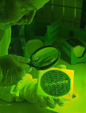
Silicon Wafer Processing
NOVA offers many wafer processing services for MEMS/NEMS and Micro-Machining projects to satisfy simple to complex requirements. We align with top industry suppliers to provide our clients high quality thick film, bonded SOI wafers, and offer trench etch and refill services on bulk silicon substrates or on SOI. By combining both SOI and trench etch and refill technology, we can offer customers a unique dielectrically isolated substrate preparation service.
Silicon Epitaxial Services
NOVA also supplies custom epitaxial layers on silicon wafers for research and development or large scale production. Our services include single layers, growth on buried layers and patterns as well as advanced device structures on wafer diameters 100mm to 200mm.
Other Services
- High Precision Dicing
- Die Processing
- Deep Reactive Ion Etching (DRIE)
- Direct Wafer Bond (DWB)
- Laser Cut Down
- Laser Marking
- Photoresist Coating - 5,000 - 30,000Å
- Photoresist Stripping - H2SO4 / H202 (Piranha), O2 Plasma
- Polishing - single side and double side
- Proximity Photolithography
- Stepped Photolithography
- Wafer Bumping
- Wafer Thinning
- Wet Cleaning - RCA, SC1 - SC2, Dilute HF/DI cleaning
- Wet Pattern Etching - HF-BOE oxide, KOH Silicon etching
NOVA understands quality and consistency are imperative to device manufacturing so we are committed to providing you top notch services you can count on at affordable prices.
Contact NOVA for more information at (972)478-7002 or submit an online Service Request.
Print This Page
NOVA offers the best competitive pricing without sacrificing quality. No order is too big or too small for us to handle. Contact Us today.