Thin Films
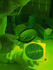
NOVA offers a wide variety of unique dielectric and conductive thin films to satisfy your MOS and MEMS process requirements. Services are available on silicon wafers as well as other materials such as quartz, sapphire and aluminum nitride.
Wet Thermal Oxide is preferred when growing thick oxide. Dry Thermal Oxide is available for those applications requiring a thinner oxide. Dry Chlorinated Thermal Oxide with Forming Gas Anneal is recommended for use in MOS and other active device fabrication processes.
| Thermal Processing (both sides) | Thickness | Diameter |
|---|---|---|
| Dry Thermal Oxide | 100 - 3000Å | 2" - 12" |
| Dry Chlorinated Thermal Oxide with Forming Gas (H2/N2) Anneal |
100 - 3000Å | 2" - 8" |
| Wet Thermal Oxide | 1000 – 60,000 Å | 2" - 12" |
| LPCVD Nitride Deposition (both sides) | Thickness | Diameter |
|---|---|---|
| Stoichiometric | 50-4500Å | 2" - 12" |
| Low Stress (stress less than 250 MPa) | 50 – 20,000 Å | 2" - 12" |
| Super Low Stress (stress less than 100 MPa) | 50 – 40,000 Å | 2" - 12" |
PECVD allows thin film deposition at lower temperatures than those found in LPCVD processing and can be useful for wafers that require minimal thermal processing.
| PECVD Processes (single side) | Thickness | Diameter |
|---|---|---|
| Nitride Deposition | 100 - 5000� | 2" - 12" |
| Nitride - Low Stress | 100 – 20,000 Å | 2" - 12" |
| PECVD Oxide | 100 – 50,000 Å | 2" - 12" |
| PECVD OxyNitride | 100 – 20,000 Å | 2" - 12" |
| PECVD Silicon Carbide | 100 - 2000Å | 2" - 12" |
| PETEOS Oxide Deposition | 500 – 30,000 Å | 8" only |
| Polysilicon Deposition | 1000 – 20,000 Å | 3" - 12" |
Contact NOVA for more information about custom films. Phone us at (972)478-7002 or submit an online Service Request.
Print This Page

NOVA offers the best competitive pricing without sacrificing quality. No order is too big or too small for us to handle. Contact Us today.
